When p orbitals do the wave
Scanning tunneling microscopy visualizes signatures of p-orbital texture in the charge-density-wave state of the topological semimetal candidate CeSbTe

The two-dimensional (2D) square lattice with degenerate px and py orbitals is a textbook model for charge density wave (CDW). Due to the anisotropic shape of the p orbitals, hopping of electrons between px orbitals occurs primarily along the x direction, whereas hopping of electrons between py orbitals occurs primarily along the y direction. The resulting Fermi surface comprises quasi-1D bands that are well nested and favorable for CDW formation. Early discussions of this model revolved around the classic “stripes vs. checkerboard” question [1]: Under which conditions should the CDW be a double-q “checkerboard” that breaks only translational symmetry, and under which conditions should the CDW be a single-q “stripe” that breaks both translational and rotational symmetries? This model is believed to offer some insights into the stripe-like tendencies of charge ordering in the cuprates and nickelates.
More recently, indications that the CDW on a p-electron square lattice can be much more exotic than checkerboards and stripes have begun to emerge. Raman spectroscopy of RTe3 (R = Gd, La), which hosts Te square lattices with 5p orbitals, has revealed the CDW state to break not only translational and rotational symmetries, but also additional mirror symmetries [2–4]. The amplitude mode of the CDW exhibits an unusual axial symmetry. The speculation is that the 2D square lattice possesses a hidden orbital degree of freedom, namely, px or py orbitals, and that the ordering of these p orbitals endows the CDW with unconventional symmetries [5]. A microscopic visualization is nevertheless necessary to confirm the real-space ordering and texture of p orbitals.
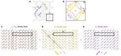
. b, Fermi surface with decomposition into orbital contributions. The CDW wave vector q is marked by the arrows. c, Pattern of bond density wave underlying the 1×7 CDW state in CeSbTe, as determined by STM. d and e, Decomposition into px and py dimer chains with periodic phase slips.")
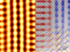
Xue et al. [6] utilize scanning tunneling microscopy (STM) to image the internal structure of the 1×7 CDW state of CeSbTe, a topological semimetal candidate comprising Sb square lattices with 5p orbitals sandwiched by magnetic CeTe buffer layers. By using an appropriate tunneling bias voltage, the authors could image electronic features from the CDW-active Sb layer, which lies two atomic planes beneath the surface. The STM image reveals atomic-sized, anisotropic lobes of charge density, whose axis of anisotropy varies periodically in space, alternating between the crystalline a and b axes (“ladder” motif). The pattern can be ultimately mapped onto a superposition of Sb 5px and 5py bond density waves that are identical in structure, but shifted in phase relative to each other, resulting in a nontrivial real-space texture.
This project was supported by the Deutsche Forschungsgemeinschaft (DFG, German Research Foundation) – TRR 360 – 492547816, “Constrained Quantum Matter” [7].
References
[1] H. Yao et al., Phys. Rev. B 74, 245126 (2006).
[2] Y. Wang et al., Nature 606, 896 (2022).
[3] D. Wulferding et al., Nat. Commun. 16, 114 (2025).
[4] B. Singh et al., arXiv:2411.08322v2.
[5] S. Alekseev et al., Phys. Rev. B 110, 205103 (2024).
[6] X. Que et al., Nat. Commun. 16, 3053 (2025).
[7] https://www.trr360.de


